


English
English
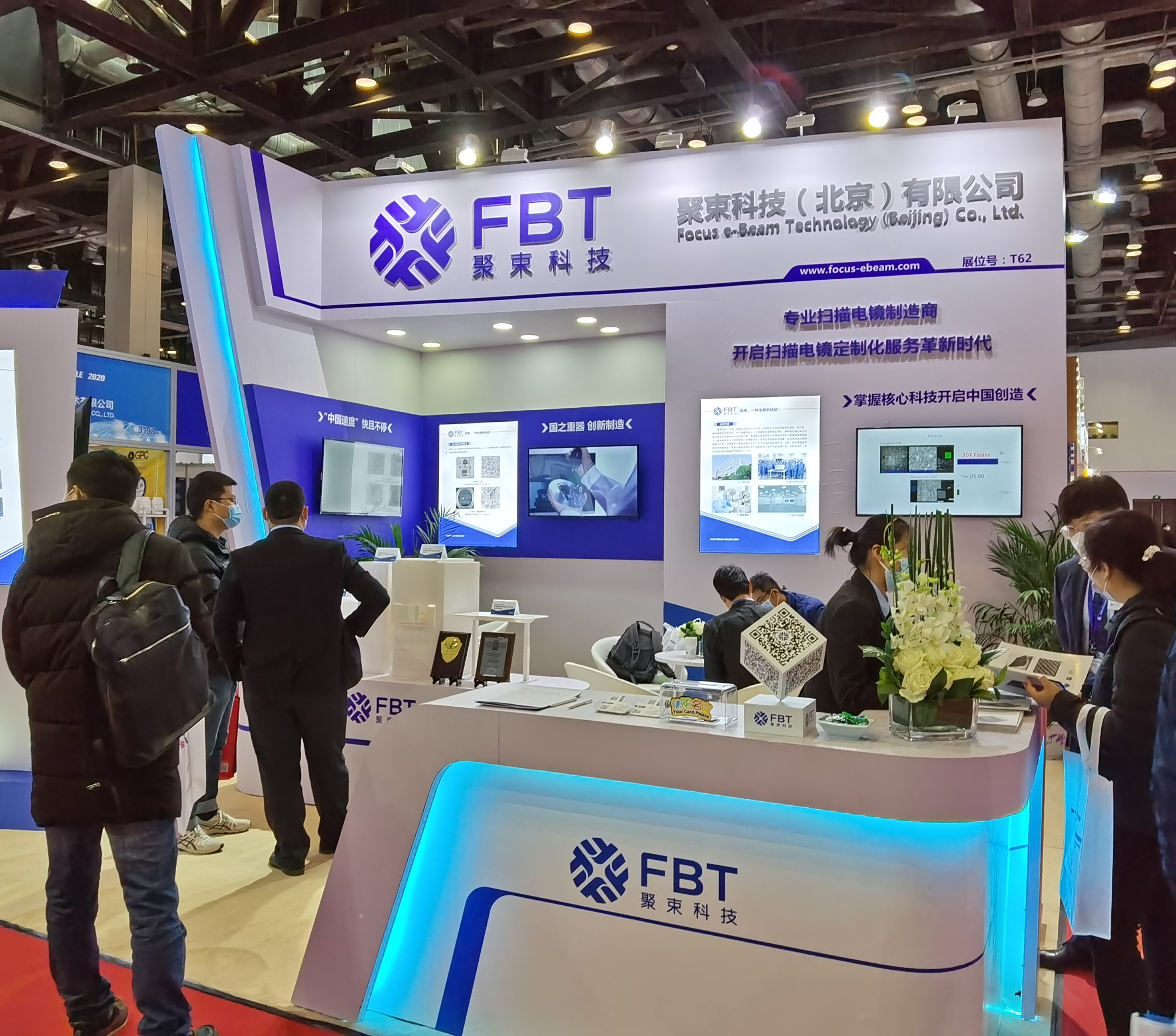
Semiconductor Industry

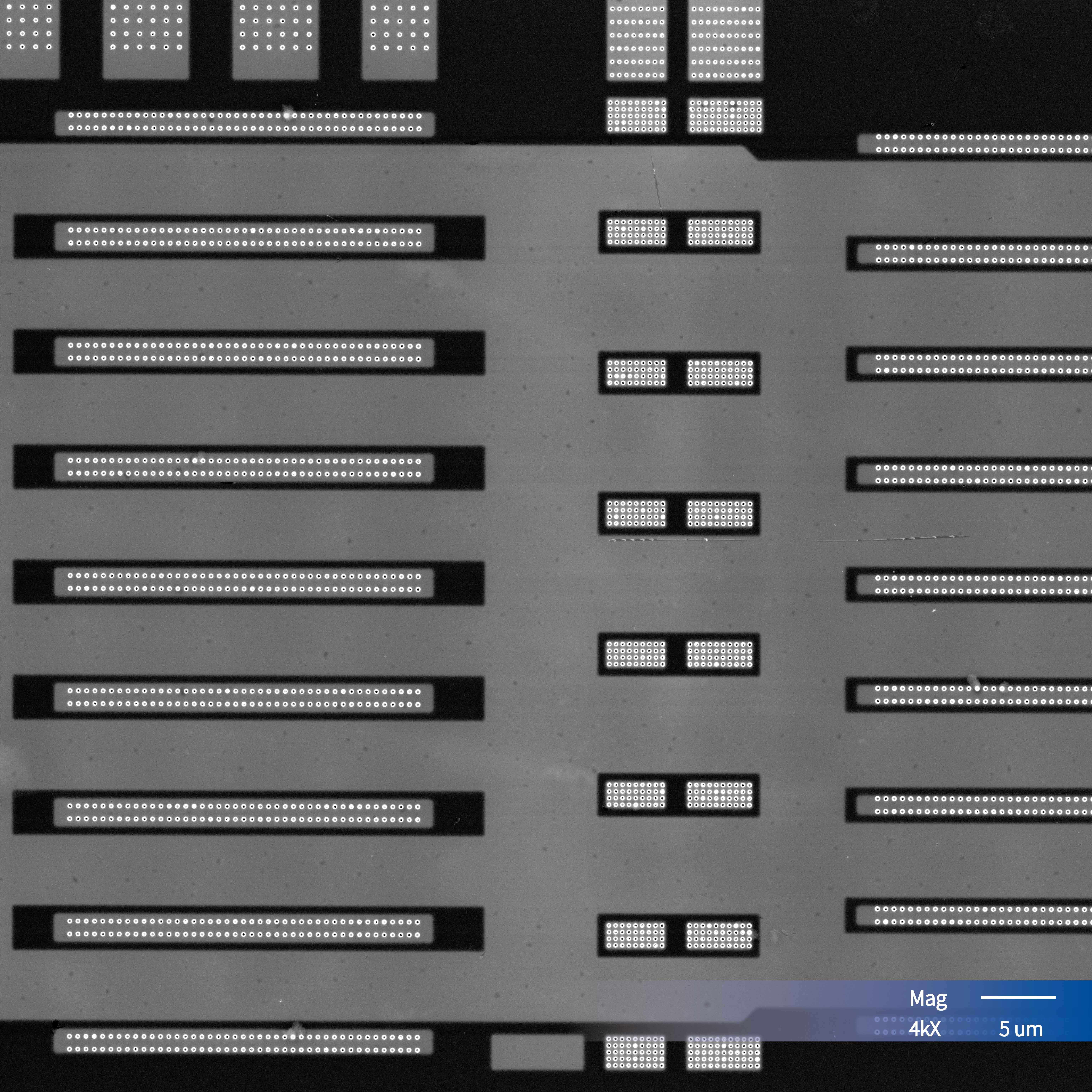
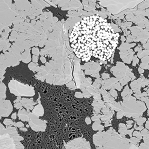
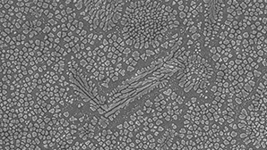
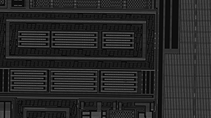
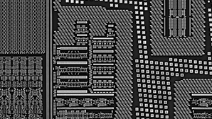
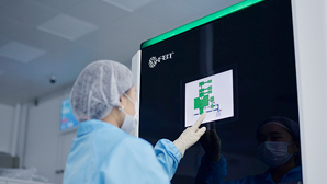
Scanning electron microscopes allows observation of the microstructure and morphology of the surface materials of semiconductor devices. Enabling real-time detection of the front structure of IC devices, integrated circuit process analysis and the cross-sectional composite structure of the device. The direct electronic detection capability and intelligent analysis software of NavigatorSEM-100 provide valuable solutions for many different applications.


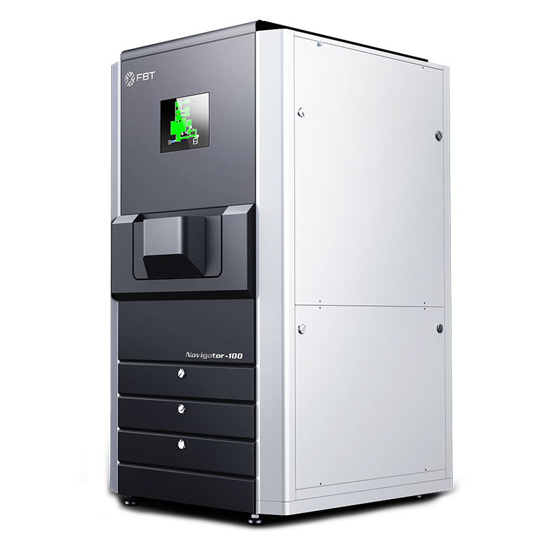
Owning our own intellectual property and propriety imaging technology, motion and circuit control. Focus e-Beam Technology produces its world's highest throughput scanning electron microscope (SEM), NavigatorSEM-100 (field emission). Enable imaging speed more than 10 times throughput of a conventional SEM. Our direct electron detection methodology overcomes traditional SEM limitations in terms of sample damage, speed and precision, upgrading SEM to a sub-nano camera. At the same time, ease of operation, fully automatic, one-key sample touch, 7*24 hours unattended operation. These improve efficiency of scientific research.
detail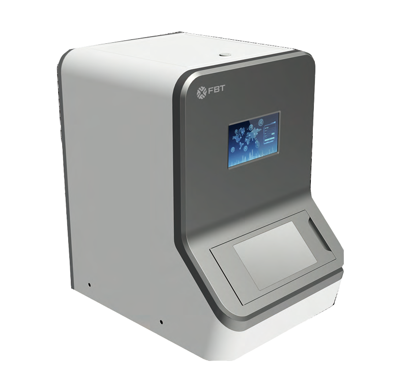
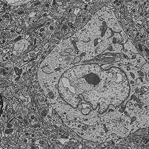
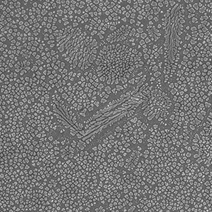
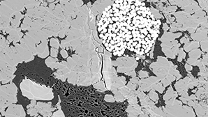
The Clippers series uses professional linear cameras with independent color processing channels to ensure more natural and accurate color reproduction and image clarity, and can easily obtain high-precision, high-quality panoramic digital slice images. One-key operation, simple and convenient. Photoelectric combination: The high-definition map scanner provide precise location to correlate and overlap the SEM coordinates. And its optical image can be used as a navigator to seamlessly connect with SEM image. Therefore, one can quickly and accurately locate and observe designated locations through the SEM. We apply mature industrial scanner technology in the semiconductor industry to life sciences, materials science, failure analysis, research and other fields. Mainly used in the research and production of ultra-large biological mesoscopic tissue structure imaging and tissue depth information, high-throughput cross-scale material characterization, large-scale sample defect screening, coating process detection, flat panel display detection, automatic particle screening, and process control.
detail